Becky
Webmistress
- Joined
- Mar 25, 2003
- Messages
- 7,424
- Reaction score
- 1,511
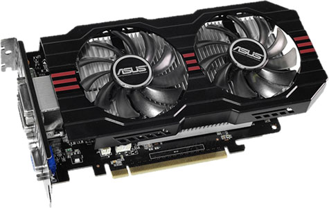
Tech Power Up have reviewed the ASUS GTX 750 Ti OC 2 GB graphics card - let's take a look:

Read more here.
"Here it is, NVIDIA's GeForce GTX 750 Ti, one of the first GPUs based on its next-generation "Maxwell" GPU architecture. First reports of the chip being based on "Maxwell" hit us by surprise as we presumed that a new micro-architecture is invariably pegged to NVIDIA's foundry partner, TSMC, to launch its next-generation 20 nanometer silicon fabrication process. The fact that TSMC's 20 nm node isn't in a position to ship out such complex ASICs as graphics processors right now and that NVIDIA wouldn't want its new architecture to in any way be hit by unforeseen issues arising out of the move to a new process may have led to the decision to use the existing 28 nanometer process.
The GeForce GTX 750 Ti and the GTX 750 (also launched today) are based on the 28 nm GM107 (GeForce-Maxwell 107) silicon. This 1.87 billion-transistor GPU features a basic component hierarchy that's not too different from that of "Kepler," but sees some under-the-hood changes in the design of its key parallel processing sub-unit, the streaming multiprocessor "Maxwell" (SMM). The GTX 750 Ti is positioned between the GTX 760 and GTX 660, which is a sizable gap to fill. NVIDIA is promising some huge performance-per-watt gains with "Maxwell." Given that the GM107 is based on the same 28 nm process as the GeForce Kepler series, there's only one way NVIDIA can deliver on its promise - by developing a better overall architecture.
Today we are reviewing the ASUS GTX 750 Ti OC, which is the first GTX 750 Ti with an additional 6-pin power connector that we've reviewed.

Read more here.
