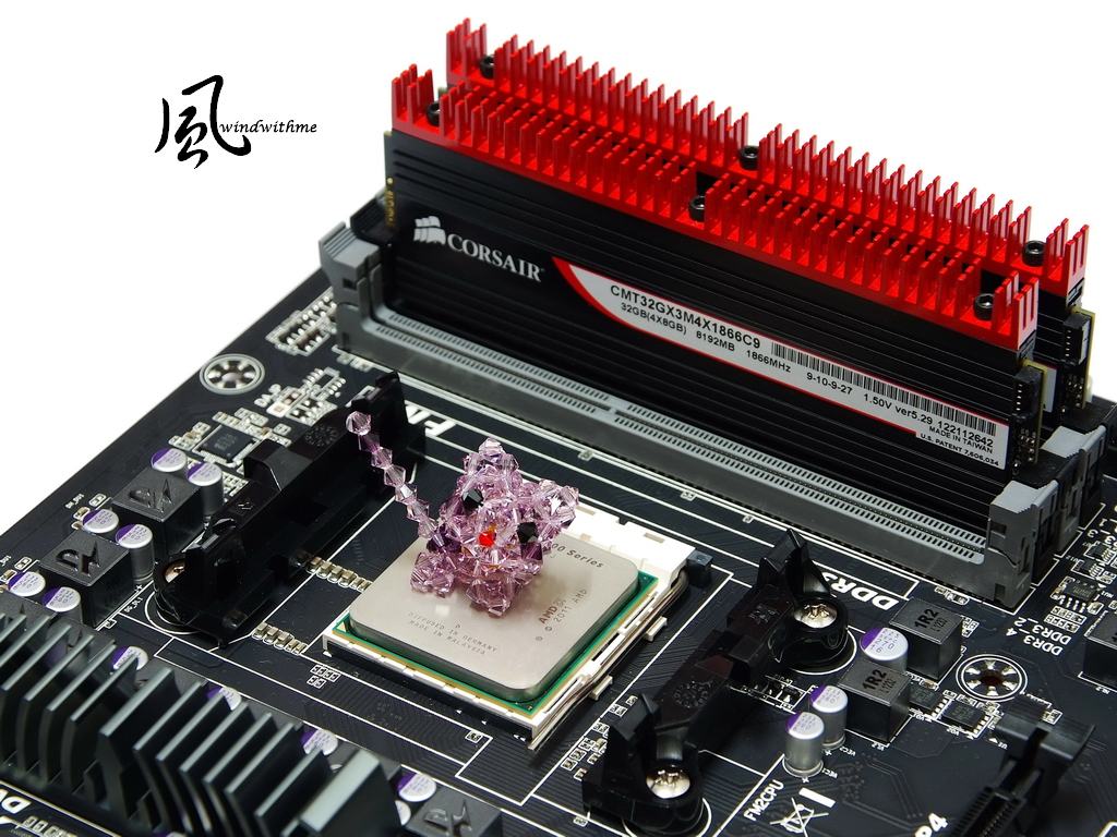
AMD A10-5800K with GIGABYTE F2A85X-UP4 OC Guide

Joined
Dec 1, 2008
Messages
730
Reaction score
47
A5800K01.jpg


AMD launched Llano APU with FM1 socket in July 2011.
Later on, AMD launched Socket FM2 in Oct 2012.
FM2 and FM1 CPU sockets are not compatible. Please be aware of it before upgrade.
In the past, the advantage of AMD platform was compatible sockets. It’s too fast for this transition.

FM2 code is Trinity APU. It combines AMD AM3+ Bulldozer structure.
The price is lower to make APU platform parity.
Chipset can use A75 and A55, but supports FM2 Socket.
AMD also launched a new chipset for Trinity APU, more high end A85X.

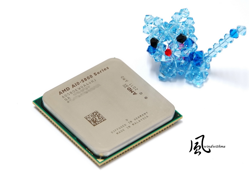
CPU is current most high end Trinity APU, A10-5800K.
32nm, 4-Cores, 3.8GHz, Turbo Core to 4.2GHz
Max TDP is 100W and built-in GPU is AMD Radeon HD 7660D
FM1 and FM2 CPU are 32nm which is no improvement in manufacturing.
A5800K02.jpg


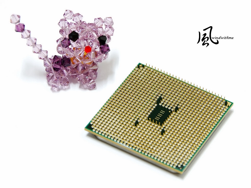
FM2 socket is 904Pin and FM1 is 905Pin.
There is one pin less as you can see in pic.
A5800K03.jpg


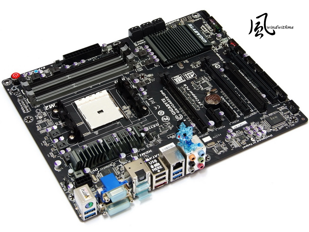
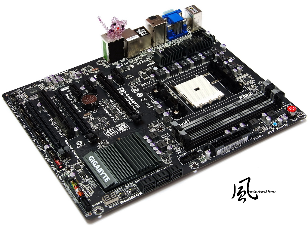
MB is GIGABYTE most high end for FM2 Socket, F2A85X-UP4
The price is just a little bit higher than A10-5800K. Building high end FM2 platform is not too costive.
It’s black and gray as main design of GIGABYTE high end MB.
A5800K04.jpg


It’s own durable design. Blink of an eye, it’s 5th generation.
2oz PCB and 60A Ferrite core choke and latest IR3550 PowIRstage chip.
In my previous review, I have shared the good temperature performance of IR3550 PowIRstage.
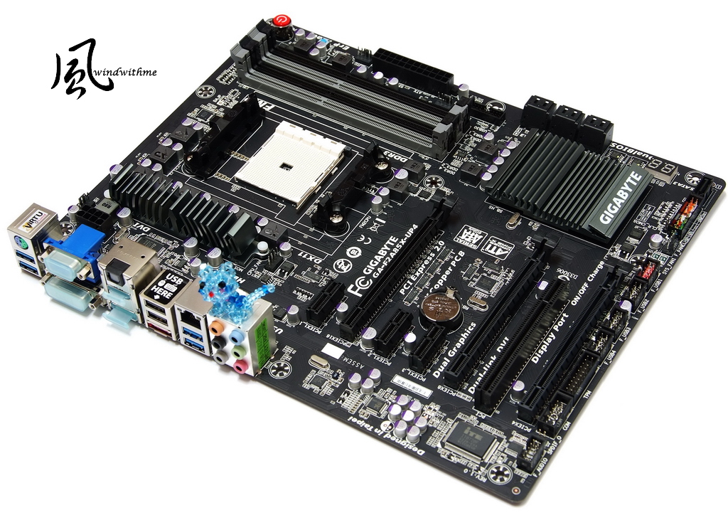
A5800K05.jpg


Lower-Left Corner
3X PCI-E X16, they are X16, X8 and X4.
Supporting AMD Dual Graphics and MD CrossFire
3 X PCI-E X1
1 X PCI
Realtek ALC892 audio supports 7.1 channels and High Definition Audio
Realtek RTL8111F LAN chip and TPM slot
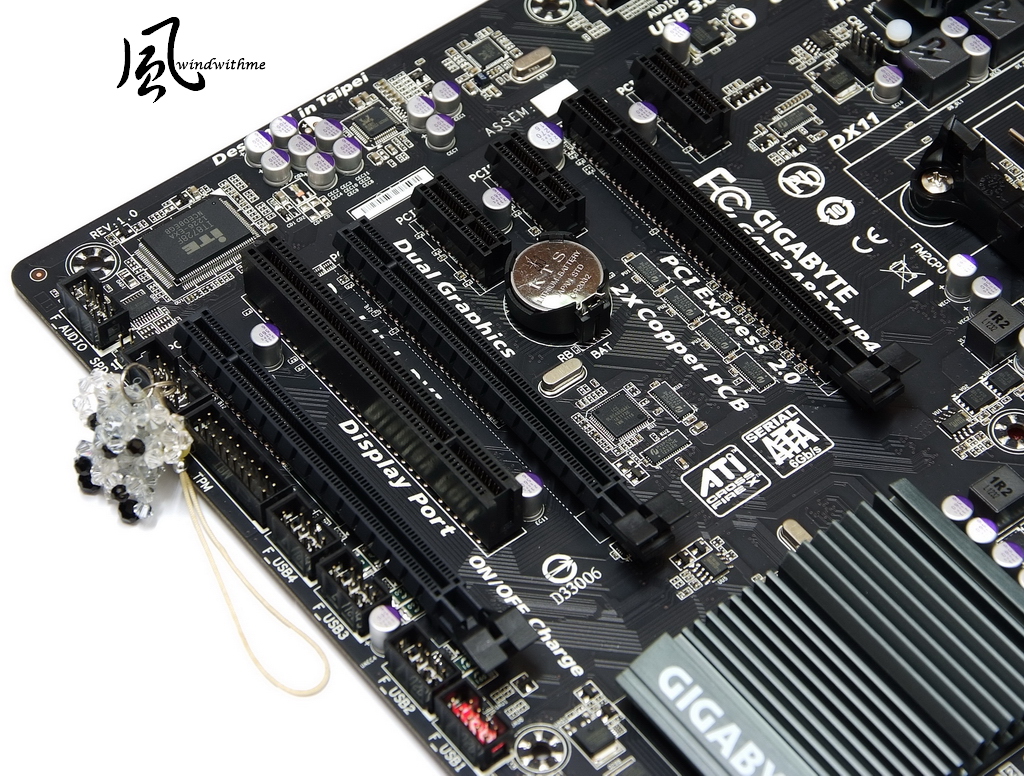
A5800K06.jpg


Lower-Right Corner
7 X Black SATA provided by A85X, supporting SATA3
It Supports RAID 0, RAID 1, RAID 5, RAID 10 and JBOD.
Right side is debug LED and dual 64 Mbit Flash BIOS
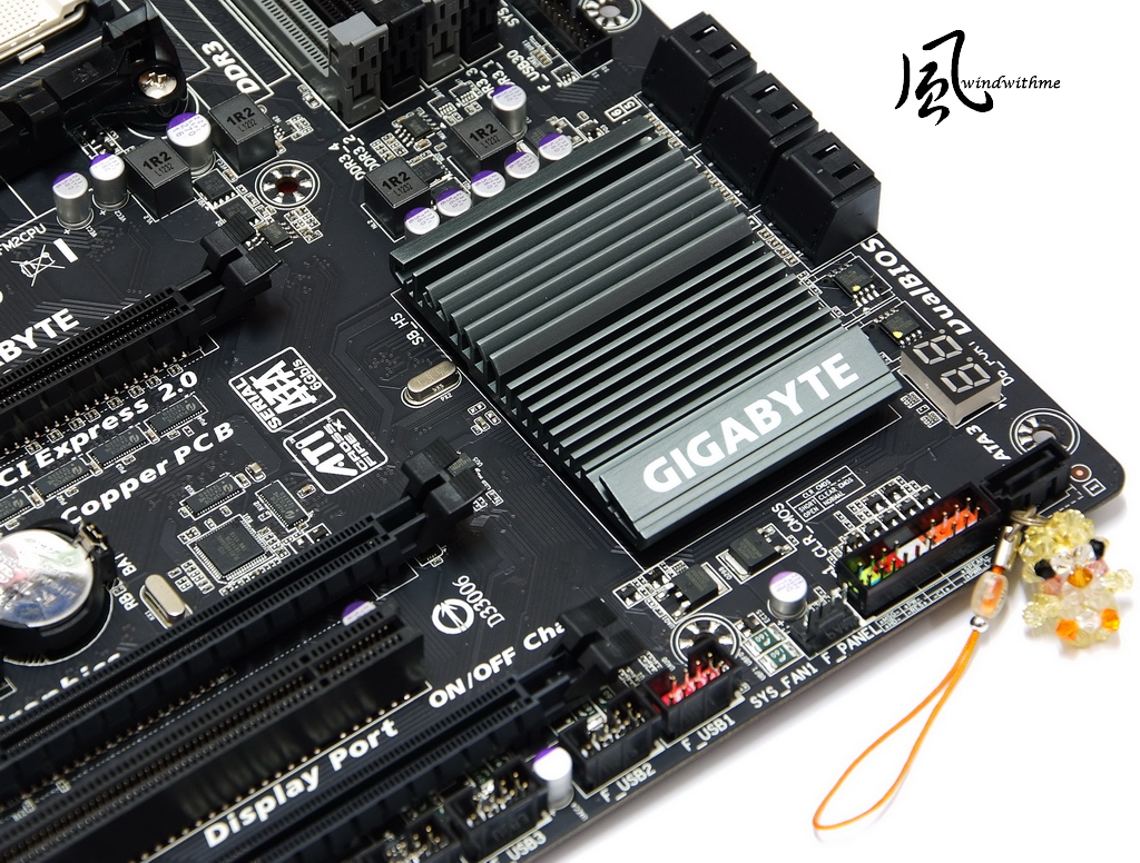
A5800K07.jpg


Upper-Right Corner
4 X DIMM DDR3 support 1066/1333/1600/1866. Max DDR3 capacity is 64GB.
It supports AMD Memory Profile / Extreme Memory Profile.
Next is 24-PIN power connector and front USB 3.0 connectors.
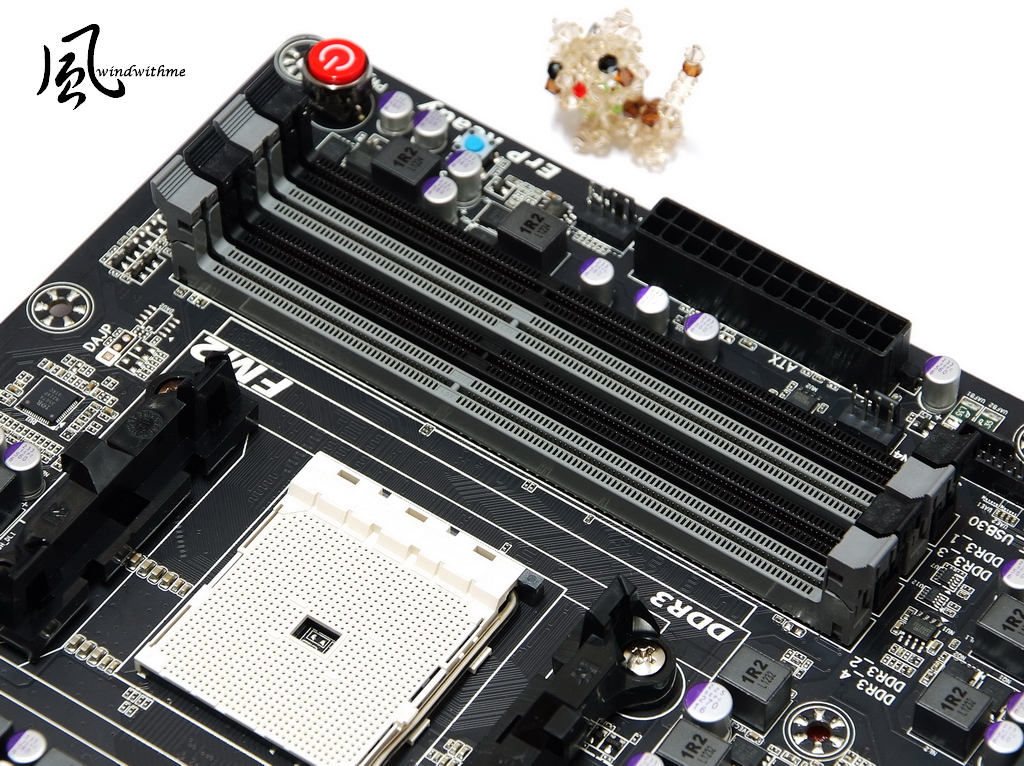
A5800K08.jpg


Upper-Left Corner
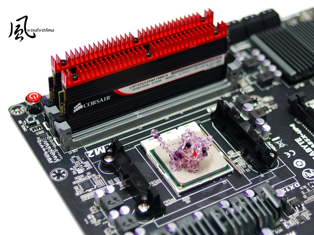
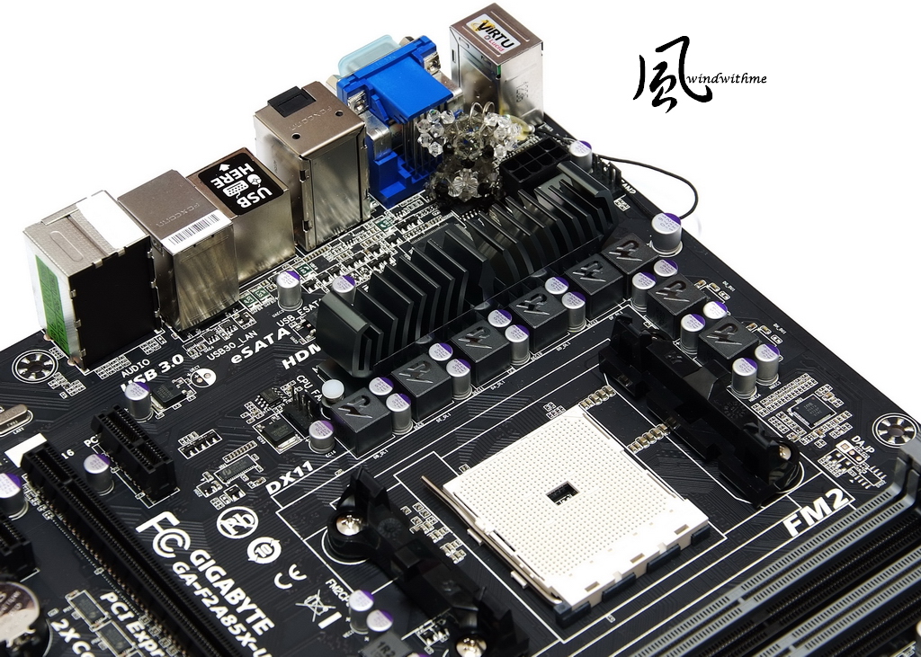
F2A85X-UP4 CPU left side is iron-gray sink. It’s 8-phase digital PWM.
Upper-left is 8Pin power connector. FM2 socket supports AMD A and Athlon series CPU
Red button is power, blue is Reset and black is Clear CMOS.
A5800K09.jpg


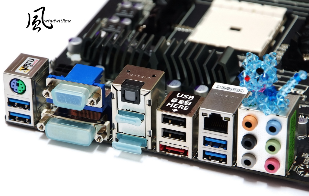
IO
1 X PS2 KB/Mouse
1 X D-Sub / DVI-D / HDMI / DisplayPort
4 X USB 3.0/2.0(Blue)
2 X USB 2.0(Black)
1 X S/PDIF optical outpur
1 X eSATA 6Gb/s Port
1 X RJ-45 LAN
6 X audio jacks
A5800K10.jpg
 
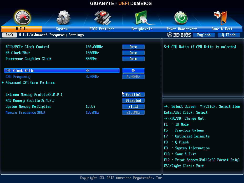
UEFI Screen
CPU Clock Ratio adjusts from 38 to 45. It means OC 5800K to 4.5GHz.
DDR3 enables Extreme Memory Profile to run at 2133.
A5800KB01.jpg


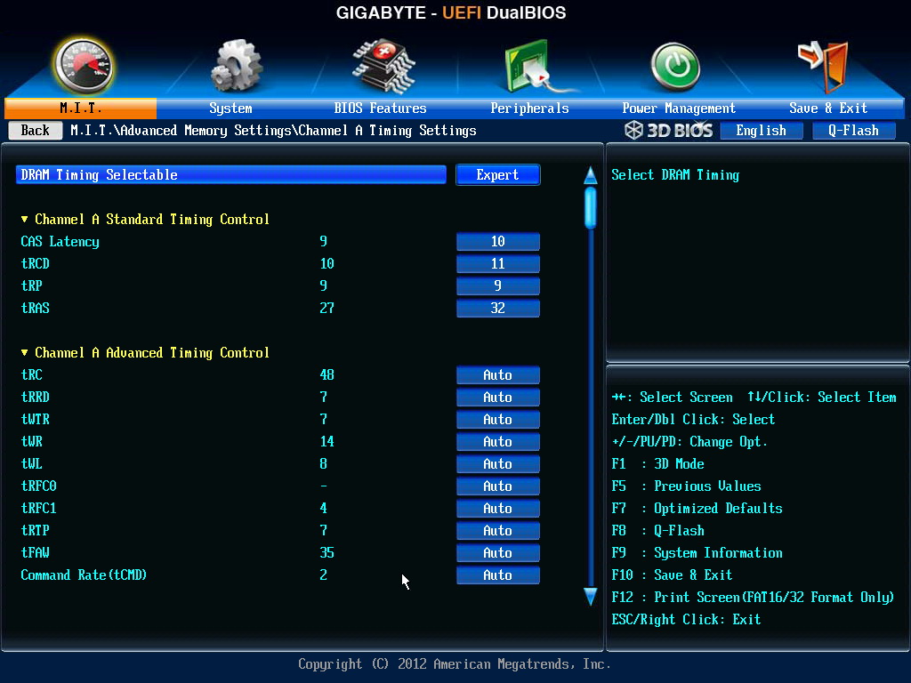
DRAM Advanced Parameters, manually setup as CL10 11-9-32
A5800KB02.jpg


Voltage Page
CPU Vcore 0.80000~2.30000V
DRAM Voltage 1.100~2.620V
CPU set as 1.46250V and DRAM set as 1.600V
A5800KB03.jpg


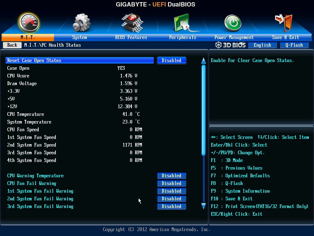
PC Health Status
As OC setup above, the CPU temperature is over 41 degree C. It’s more accurate in UEFI temperature info.
As CPU temperature, I will have further test later.
A5800KB04.jpg


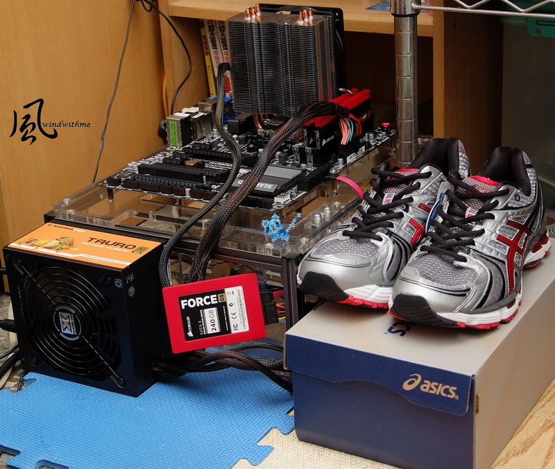
Test Configuration
CPU: AMD A10-5800K
MB: GIGABYTE F2A85X-UP4
DRAM: CORSAIR DOMINATOR-GT DDR3 1866 8GX2
VGA: AMD Radeon HD 7660D
HDD: CORSAIR Force GS 240GB
POWER: XIGMATEK Tauro 400W Bronze
Cooler: XIGMATEK HDT-S1283
OS: Windows8 64bit
A5800K11.jpg


Performance Test
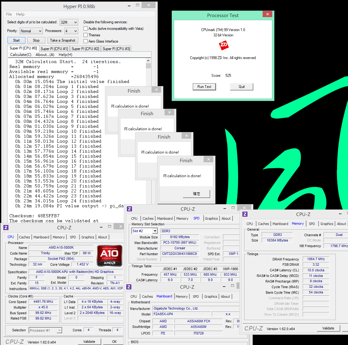
CPU 99.82 X 45 => 4491.76MHz
DDR3 2129.4 CL10 11-9-32

Hyper PI 32M X 4 => 24m 19.084s
CPUMARK 99 => 525
A5800KOPI.png


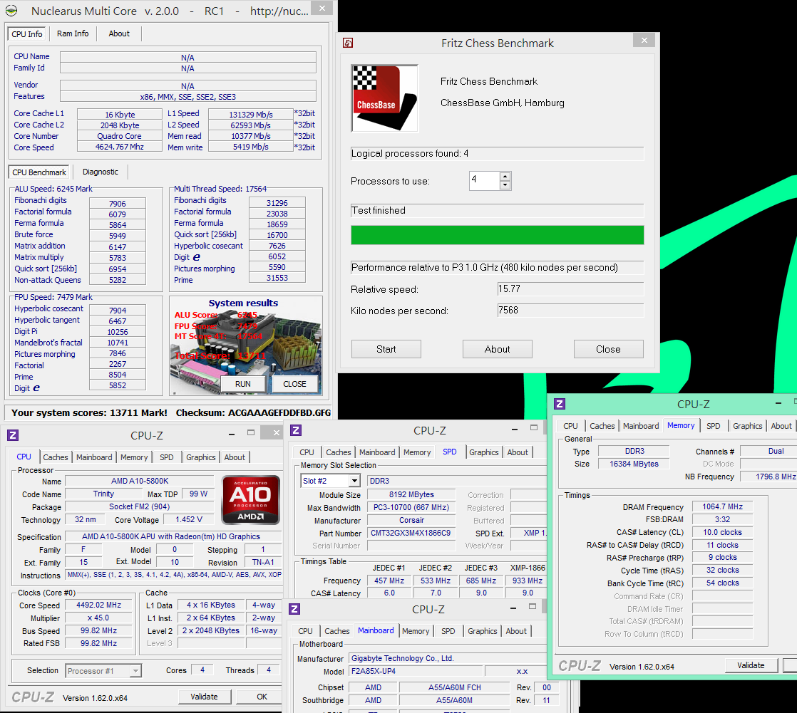
Nuclearus Multi Core => 13711
Fritz Chess Benchmark => 15.77/7568
A5800KONM.png


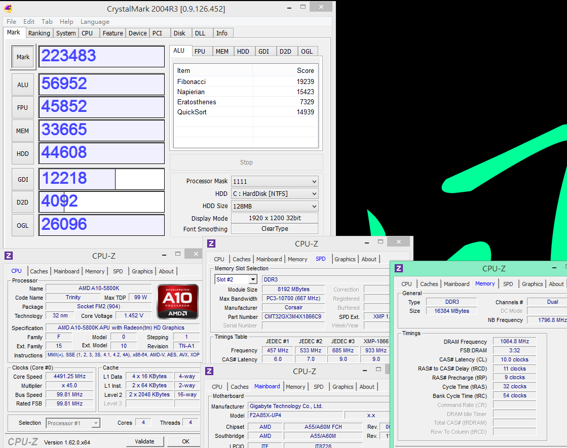
CrystalMark 2004R3 => 223483
A5800KOCM.png


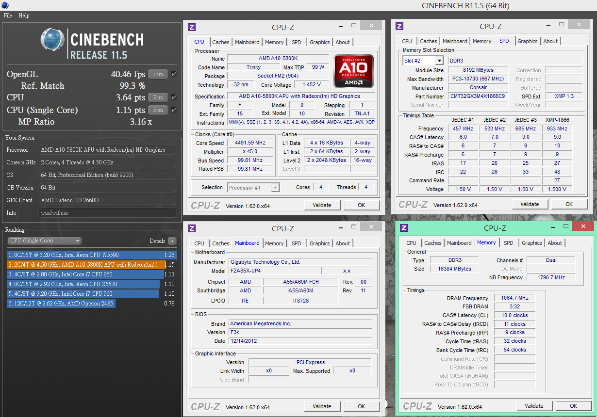
CINEBENCH R11.5
CPU => 3.64 pts
CPU(Single Core) => 1.15 pts
A5800KOCB.png
 
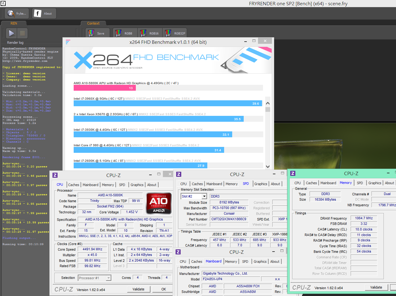
FRYRENDER
Running Time => 10m 39s
x264 FHD Benchmark => 13
A5800KOFRY.png


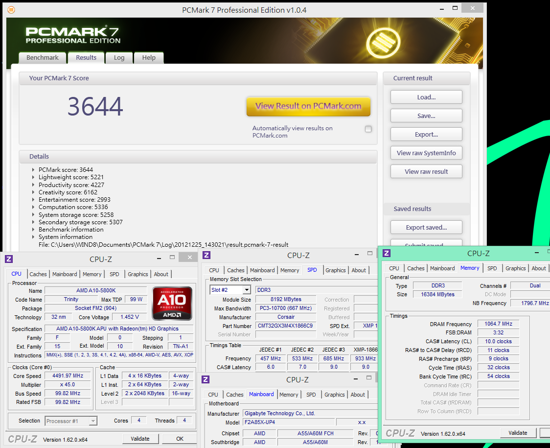
PCMARK7 => 3644
A5800KOPC7.png


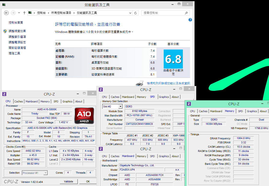
Windows8 Experience Index - CPU 7.4
A5800KOWIND8.png


FM2 5800K clock after OC is much higher than FM1 3850.
As 5800K using dual module quad core structure, the clock and OC ability are improved a lot.
If we just look at performance in CINEBENCH, the CPU single and multiple threads numbers are as below.
FM2 5800K OC 4492MHz and i3-3220 default 3293MHz.
i3-3220 Single Core CPU is 26.2% higher, and 5800K multi-CPU is 14.5% higher.
FM2 5800K OC 4492MHz and FM1 3850 OC 3540MHz
3850 Single Core CPU is 14.8% higher and 5800K multi-CPU is 7.4% more.
As multi-tasking Fritz Chess Benchmark, these 3 CPUs performance is similar.
It’s up to your requirement to decide which one is more suitable for you.

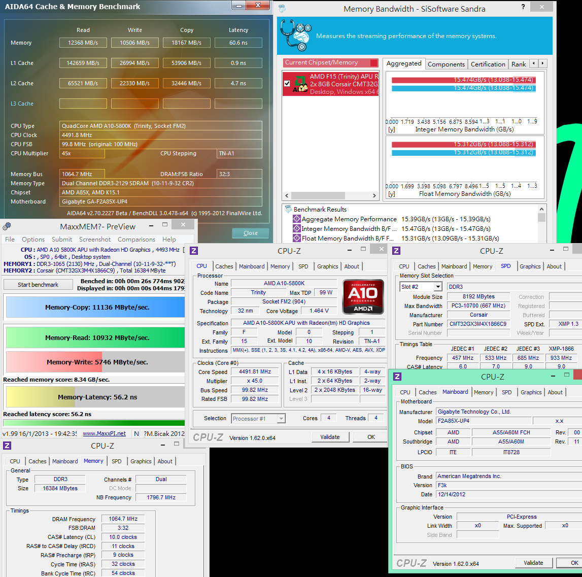
2134.8 CL10 11-9-32
ADIA64 Memory Read - 12368 MB/s
Sandra Memory Bandwidth - 15474 MB/s
MaXXMEM Memory-Copy - 11136 MB/s
A5800KOMEM2133.png


FM2 default clock can pull to 2133 which is higher than FM1 1866.
In ADIA64 Memory Read, the bandwidth increases 20%.
However, in Sandra and MaXXMEM, it’s lower than FM1.
As new structure characteristic and bandwidth performance, you can decide by high clock or bandwidth.

3D Performance Test
Built-in AMD Radeon HD 7660D
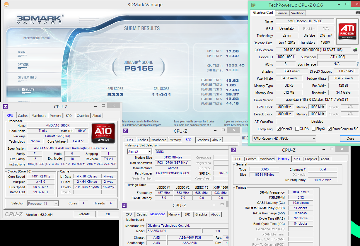
3DMark Vantage => P6155
A5800KO3DVAN.png


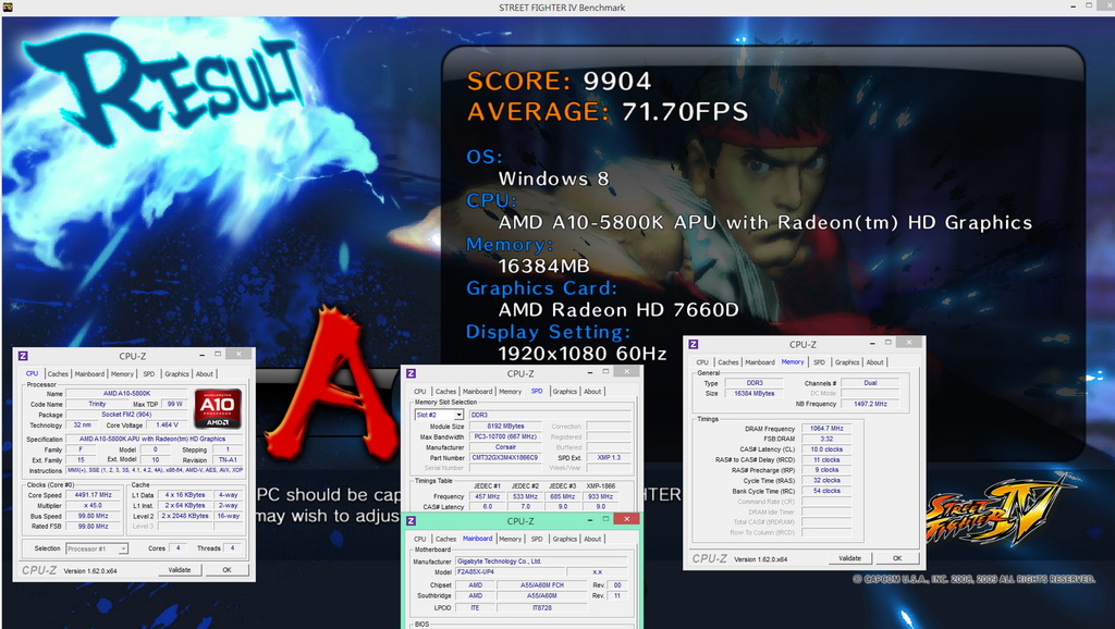
StreetFighter IV Benchmark
1920 X 1080 => 71.70 FPS
A5800KO3DSTF4.jpg


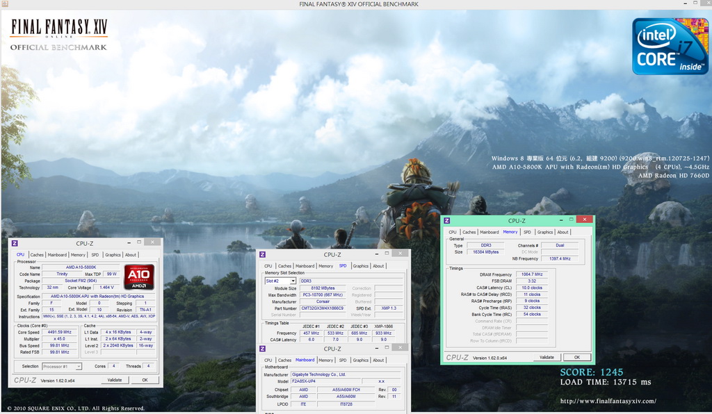
FINAL FANTASY XIV
1920 X 1080 => 1245
A5800KO3DFF14.jpg


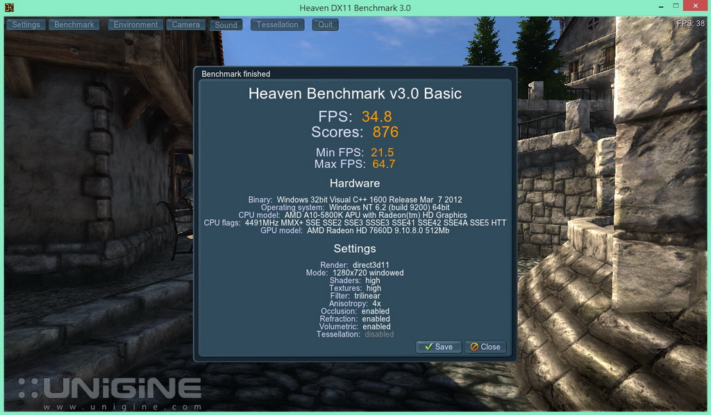
Unigine Heaven Benchmark
1280 X 720 => 34.8 FPS
A5800KO3DHB3.jpg


3DMark Vantage is 20% higher than previous Radeon HD 6550D with 3850.
StreetFighter IV Benchmark and FINAL FANTASY XIV performance is similar.
However, Unigine Heaven Benchmark test DX11, it’s almost double the 3D performance.
5800K built-in AMD current most high end Radeon HD 7660D, the 3D performance is excellent.
This is the advantage of AMD APU platform. It’s designed for pull high built-in 3D performance for entry 3D demand users.

SATA3 Test
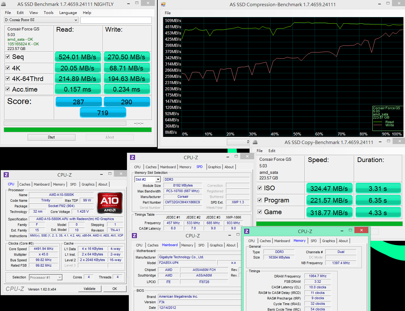
SSD is CORSAIR Force GS 240GB
AS SSD Benchmark - 719
Seq Read - 524.01 MB/s Write - 270.50 MB/s
4K - 64Thrd Read - 214.89 MB/s Write - 194.63 MB/s
A5800KOSSD1.png


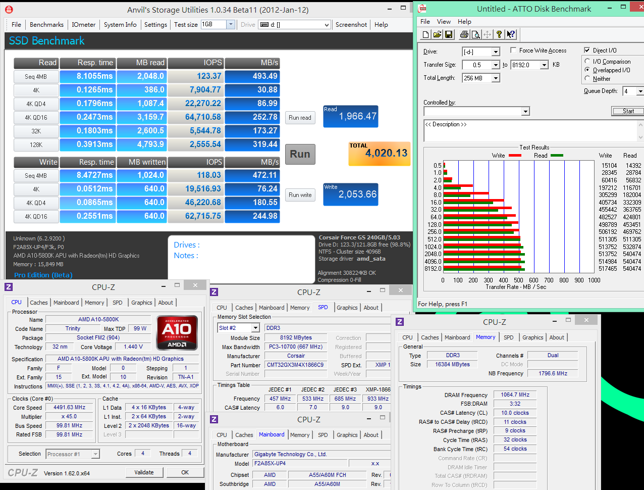
ATTO DISK Benchmark over 512KB test can reach 540.5 Mb/s read and 517.5 MB/s write.
SSD Benchmark TOTAL => 4020.13
A5800KOSSD2.png


Trinity APU latest A85X chipset supports 8 native SATA3 ports.
For users who own many HDD o SSD, the transfer rate is a key factor.
In the past, AMD SATA transfer rate is not as good as Intel. However, it improves step by step.
Form the test above, you can see overall read/write performance and 4K - 64Thrd are both in good level.
However, for 4K read/write performance is only 50~60% of Intel chipset. It must improve in the future.
Also as SSD Raid 0 Trim technology and performance, I hope AMD new chipset can catch up as well.
 
Temperature(Room is 22˚C)
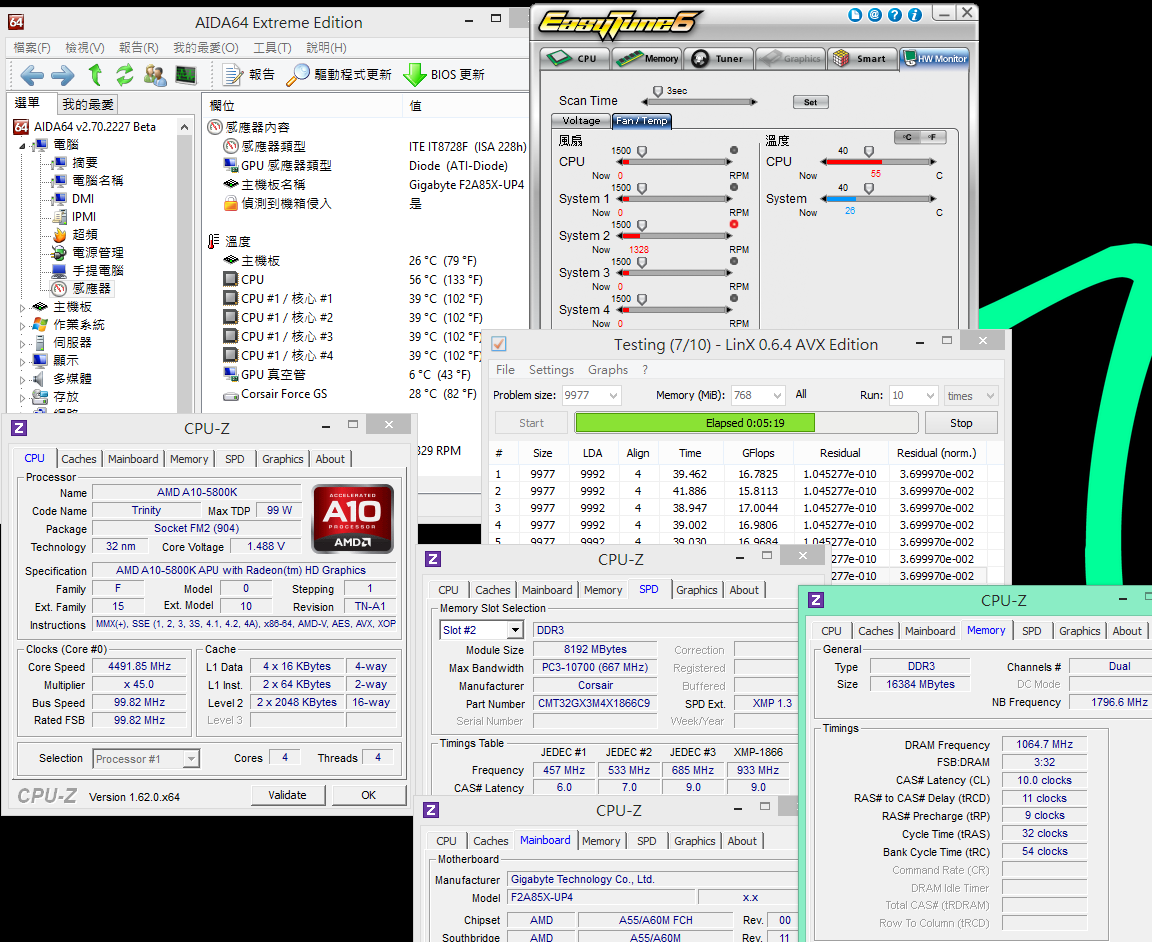
Enter to OS Desktop - 40
A5800KOT1.png


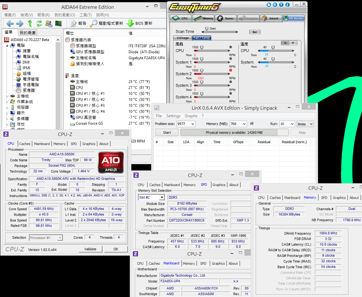
CPU Full Speed - 55
LinX 0.6.4
A5800KOT2.png


Disabling AMD C&Q power saving feature do testing. 32nm APU and FX CPU are low temperature in most software.
Sometimes, even lower than room temperature, like 8~16. As CPU is not thermoelectric Cooling, it should be higher than room after power on.
It’s impossible numbers, so just ignore the AIDA.
As EasyTune6, CPU temperature is 55 as full speed which is quite good with mid end cooler.
As 32nm, the temperature performance is good. I recommend you to use MB bundle software or UEFI BIOS to check the accurate temperature.

Power Consumption
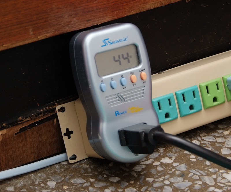
Enter to OS Desktop - 44W
A5800KWIDLE.jpg


CPU Full Speed - 165W
LinX 0.6.4
A5800KWLINX.jpg


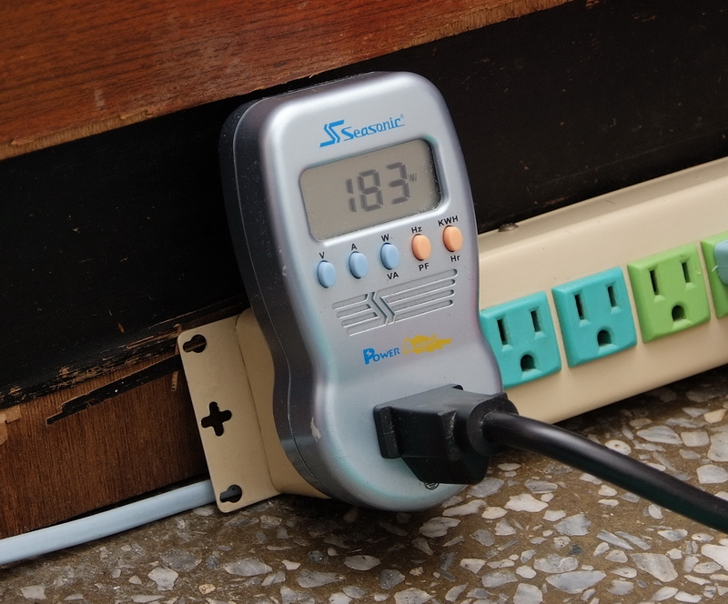
CPU and GPU both Full Speed - 183W
OCCT Power Supply Test
A5800KWOCCT.jpg


Even disable AMD C&Q power saving technology, it’s only 44W as OC to 4.5GHz.
CPU full speed is 165W which still too high. GPU full speed only increase 18W is very good.
Power consumption is weakness for AMD. Finally, it moves to 32nm, but the power consumption doesn’t decrease efficiently.

GIGABYTE F2A85X-UP4
Pros
1. Black PCB with good quality. Trinity APU structure makes high end MB parity.
2. Using IR3550 PowlRstage PWM to lower MOSFET tmeperature
3. 7 SATA3 and 1 eSATA3 for better expandability
4. IO has 4 different video output ports and supports 4 USB 3.0 devices
5. Build in debug LED and 3 buttons for bare system users

Cons
1. CPU full speed power consumption is too high
2. Better to have 2 PCI slots

A5800K12.jpg


Performance ★★★★★★★★☆☆ 81/100
Components ★★★★★★★★★☆ 86/100
Specifications ★★★★★★★★★☆ 88/100
Appearance ★★★★★★★★☆☆ 83/100
C/P Value ★★★★★★★★☆☆ 82/100

As the test above, you can see the difference between FM2 Trinity APU and FM1 Llano APU.
Trinity APU advantage is CPU clock can pull high and DDR3 clock is one level higher as well.
Temperature and power consumption are similar as they are both 32nm.
5800K built-in 3D performance improves a lot, especially in DX11 supported games.

A5800K13.jpg


Latest Trinity APU still focus in mid to low end market to provide more parity options.
New chipset specs are better than A75 and supporting more SATA3.
If you own FM1 already, you don’t really need to upgrade to FM2.
If you are planning to buy a new entry PC and require 3D performance more than CPU, Trinity APU can be a good choice for you :)

This article is also post in my blog - WIND3C, Any comments are welcome.
 
Back
Top